
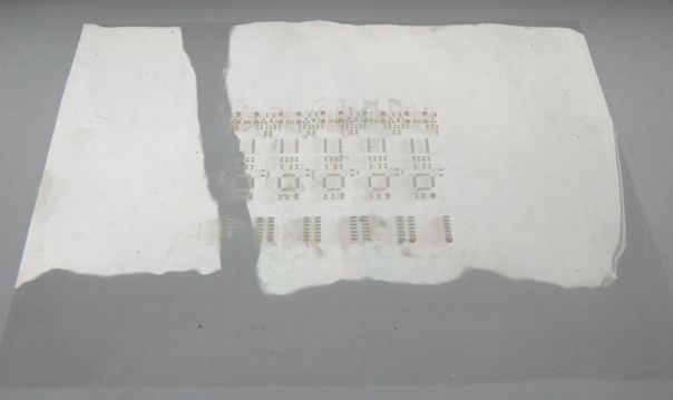
Just received the new solder paste stencil from Pololu, it’s laser-cut from 3 mil mylar sheet:
Great, once all the parts are in I can try out the new JeeNode USB v3 boards and start “baking” a couple!
Just received the new solder paste stencil from Pololu, it’s laser-cut from 3 mil mylar sheet:
Great, once all the parts are in I can try out the new JeeNode USB v3 boards and start “baking” a couple!
Comments are closed.
Theme: DePo Masthead by Derek Powazek
It just occurred to me : you said that the RTC battery had problems with some mask being too high in relation to a soldering pad. If you can raise that difference a bit more, you have pools to wipe paste into right on the PCB. so that would eliminate these stencils…
Wow… what a brilliant idea! Need to think about the holes though – all the PCBs have holes for connectors and through-hole parts. Perhaps cover them up somehow? Or apply very selectively with a very narrow strip? Maybe the PCB houses can apply a second layer of … something, to cover the holes?
If we can solve that, the solder paste stencil could be dispensed with altogether. That would be fantastic! A “game changer” as they say, these days :)
well, for starters the stencil could be just covering the connectors on the side; just sticky tape would do, as you only need to cover while applying paste. is it even a problem that through-holes are tinned ? (thinking about it : is tinning of the pads not offered by the pcb manufacturer? in that case it might be enough to just heat the pcb and dispense with the paste) sorry if I lead you astray, I have no personal experience with smd/reflow soldering. Use what seems usable ;-)
you could try what a white border around each pad would mean in added height (i.e. the stuff you write the pin numbers with).